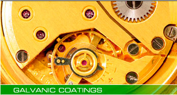
» GILDING
» SILVER PLATING
» NICKEL-PLATING
» TINNING
» ANODIZING OF ALUMINUM
» OTHER |
|
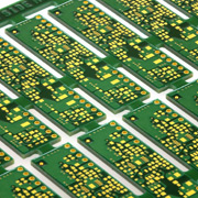
CHEMICAL GILDING OF PRINTED CIRCUITS

| |
|
 |
 Maximum dimensions: Maximum dimensions:
The maximum dimension of the circuit for chemical gilding is 40x35 cm. |
 |
The parameters of the coat:
Thickness of the coat - 0,05-0,1 µm, on the chemical nickel subcoat (pure gold without additions). |
|
Requirements:
The circuits to be gilded cannot be covered by tin-lead coat. Not every anti-soldering layer stands the process of chemical gilding. |